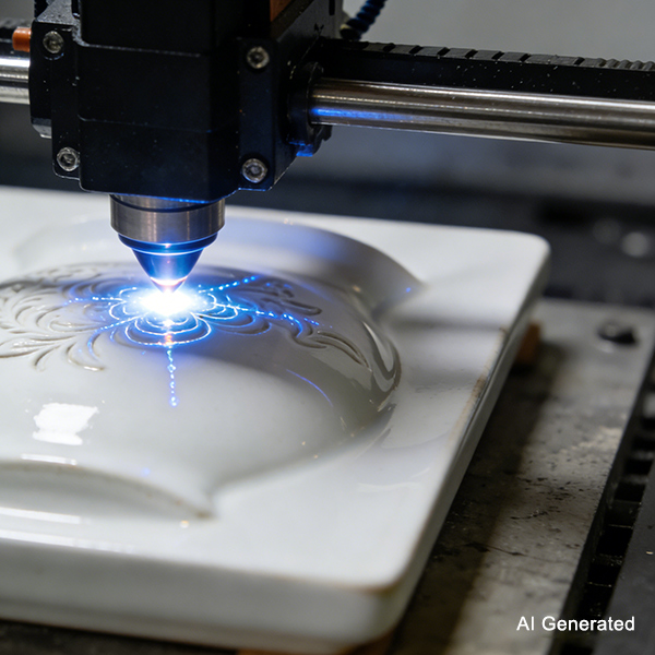
01 Introduction
Ceramic materials exhibit high thermal conductivity, low dielectric constant, and excellent mechanical strength, demonstrating outstanding heat dissipation and stability in electronic applications. However, controlling the electrical conductivity of ceramics has become a major challenge for their engineering and industrial implementation. Therefore, exploring improvements in the physicochemical properties of ceramics and surface metallization technologies has become a key driving force for the rapid advancement of electronic ceramic devices. Among existing surface treatment methods, laser surface activation and metallization have attracted significant attention due to their high precision, high efficiency, environmental friendliness, and ease of industrialization. Selective laser ablation of ceramic substrates enables surface metallization and enhances the surface conductivity of the ablated regions. Laser ablation of ceramic surfaces is a non-contact and environmentally friendly process (without toxic chemical waste) and offers extremely high precision. These advantages facilitate precise control of circuit board dimensions and optimization of circuit architectures, making this technology an ideal choice for microfluidic chip fabrication.
02 Influence of Laser Processing Parameters on the Microstructure of Ceramic Surfaces
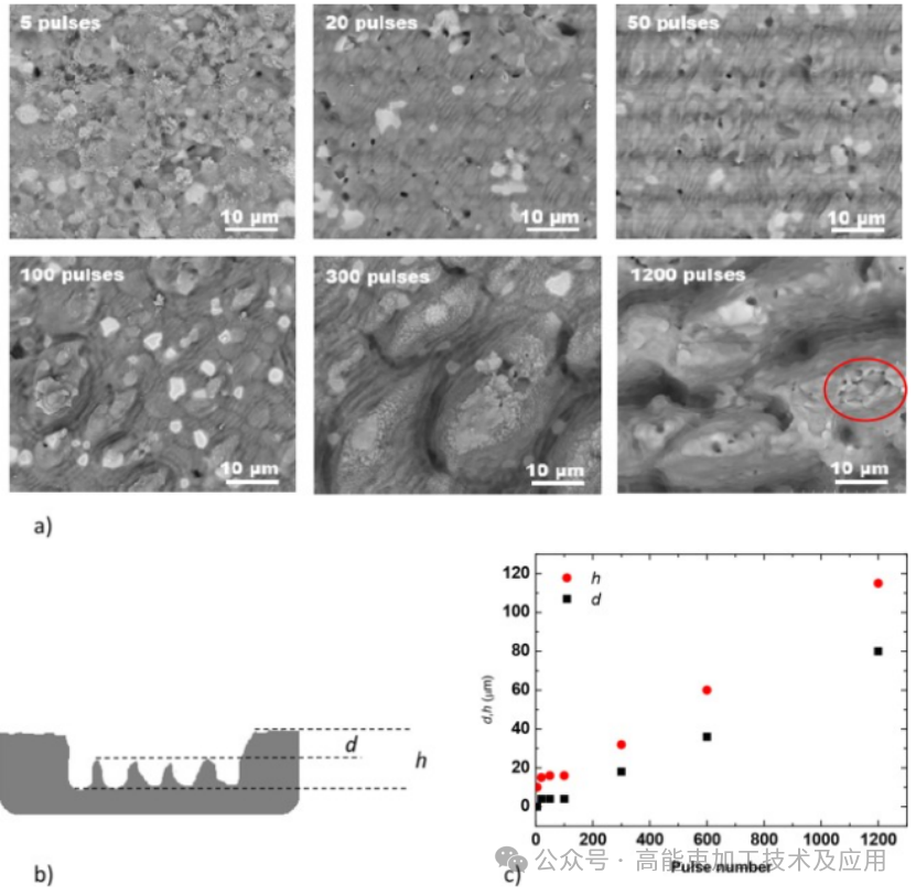
During laser ablation, ceramics undergo rapid melting, vaporization, and instantaneous rapid cooling, resulting in various surface microstructures such as grooves, pores, cracks, and recast layers. Laser activation decomposes localized precursor films on ceramic surfaces, and the decomposition products are embedded into the substrate to catalyze electroless plating layers. Studies have shown that laser surface modification can significantly enhance coating adhesion. Engineered surface topography not only increases interfacial contact area but also promotes favorable stress distribution at the interface, thereby improving the mechanical performance of the treated materials. Different laser energy distributions have a significant impact on surface morphology. When a uniform energy distribution is applied, the solid–liquid boundary of the molten pool remains relatively flat. However, when a Gaussian laser energy distribution is used, temperature gradients exist on the material surface, causing molten material to flow from the center toward the edges and leading to pronounced surface deformation. As the heating time increases, Gaussian-distributed lasers are more favorable for material removal. In addition, laser ablation can be used to generate complex patterns on ceramic surfaces, providing novel and specialized functional surfaces. N. Edyalkov et al. investigated the effects of laser energy density and pulse number on ablation depth and ablation morphology by treating AlN surfaces with nanosecond lasers, as shown in Figure 1. The ablation depth depends on laser intensity and pulse number, while ablation efficiency decreases with increasing laser intensity and pulse number.
![]()
Figure 1. Effect of different pulse numbers on the surface morphology of AlN ceramics after laser ablation [1].
03 Influence of Laser Processing Environment on the Microstructure of Ceramic Surfaces
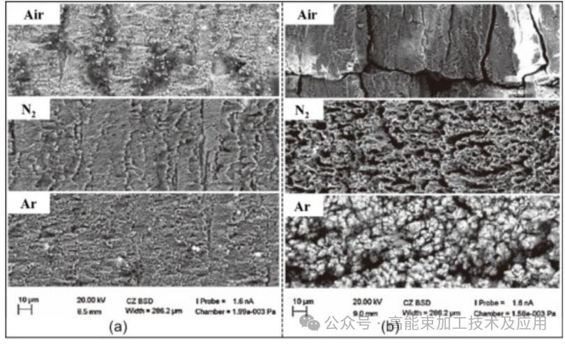
Surface engineering of materials can reduce friction and regulate wear, thereby extending the service life of mechanical systems while improving their operational performance. In laser micromachining, thermal accumulation around the heat-affected zone often leads to defects such as ripples and microcracks. In contrast, controlled thermal management plays a critical role in surface structure design during laser ablation of ceramics. By optimizing laser parameters and controlling the processing environment, the formation of microcracks can be mitigated. As energy increases, microcracks appear in the metal layer, while larger agglomerates and more pronounced porosity are observed under nitrogen and argon protection. Figure 2a shows the structure obtained when the laser fluence is close to the ablation threshold, while Figure 2b shows the structure obtained when the laser fluence is far above the ablation threshold. In an air environment, microcracks appear on the processed surface, whereas in argon and nitrogen environments, the agglomerates exhibit porous structures and the Al₂O₃ content is significantly reduced.
![]()
Figure 2. SEM images of the surface morphology of alumina-based ceramics under different gaseous environments: (a) laser flux below the ablation threshold; (b) laser flux exceeding the ablation threshold [2].
04 Influence of Laser Composite Processing on the Microstructure of Ceramic Surfaces
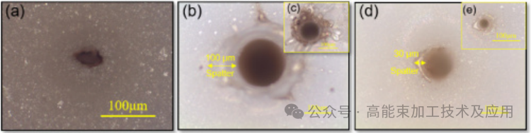
Due to their superior mechanical and physical properties, ceramics are widely used as electronic substrates. With the continuous increase in modern electronic technology demands, traditional mechanical methods or single-pulse processing techniques can no longer meet the industrial efficiency requirements for processing high-hardness ceramics. Therefore, to improve laser processing efficiency and quality, X. S. Jia et al. proposed a novel composite laser pulse (CLPs) processing method composed of millisecond pulses combined with auxiliary nanosecond pulses, as shown in Figure 3. Under the same total energy, the peak intensity of composite laser pulse trains is two orders of magnitude lower than that of conventional millisecond lasers. Enhanced interactions between millisecond and nanosecond pulses were observed to promote rapid keyhole formation. In addition, recoil pressure generated by high-intensity laser pulses or high-impact pressure produced by plasma ignition can further enhance surface material removal efficiency. When using the nanosecond–millisecond dual-component method and composite laser pulse processing, the absorption efficiency of Al₂O₃ remains within the range of 0.8–1.0, effectively avoiding absorption fluctuation issues and reducing processing losses, thereby producing hole diameters closer to the laser spot size.
![]()
Figure 3. OM images of ns pulse, ms pulse, and CLP-drilled boreholes [3].
05 Conclusion
With the development of laser technology, laser ablation is increasingly used as a surface pretreatment method prior to bonding due to its advantages of high precision, reduced circuit board size, and optimized circuit architecture, particularly for microfluidic circuit fabrication. This technology enables the formation of micro- and nanostructures on material surfaces while simultaneously modifying their chemical composition. Compared with traditional surface treatment methods, laser processing offers advantages such as low energy consumption and environmental friendliness. Moreover, it is applicable to most materials, and the fabricated micro- and nanostructures can be customized during the design and manufacturing process.
References:
[1] N. Nedyalkov, A. Dikovska, R. Nikov, R. Nikov, T. Dliov, G. Atanasova, L. Aleksandrov, D. Karashanova, V. Strijkova, M. Terakawa Nanosecond laser-induced oriented periodic structures on AlN ceramic Appl. Surf. Sci., 585 (2022), 10.1016/j.apsusc.2022.152712.
[2] D. Triantafyllidis, L. Li, F.H. Stott The effects of laser-induced modification of surface roughness of Al2O3-based ceramics on fluid contact angle Mater. Sci. Eng. A, 390 (1–2) (2005), pp. 271-277, 10.1016/j.msea.2004.08.016.
[3] X.S. Jia, G.Z. Zhu, Y.D. Zhang, Y.Q. Chen, H.L. Wang, P. Shan, K. Aleksei, X. Zhu Laser processing of alumina ceramic by spatially and temporally superposing the millisecond pulse and nanosecond pulse train Opt. Express, 28 (1) (2020), pp. 6676-6684, 10.1364/OE.381605.
**--Cite the article published by 高能束加工技术 on January 8, 2026, in the WeChat public account "High-Energy Beam Processing Technology and Applications."