01 Introduction
With the continuous advancement of science and technology and the widespread application of novel materials, modern manufacturing is rapidly evolving toward lightweight design, miniaturization, and high precision. In fields such as microelectronics, optoelectronics, and micro-electro-mechanical systems (MEMS), the interconnection and integration of micro- and nano-scale structures are particularly critical. Traditional processing methods, such as long-pulse laser processing or electrical discharge machining, are often accompanied by significant heat-affected zones (HAZ), which can easily cause material deformation, microcracks, or recast layers, making it difficult to meet the high-precision interconnection requirements at the micro- and nanoscale.
Ultrafast lasers, typically referring to lasers with pulse durations in the femtosecond (fs) or picosecond (ps) range, provide new solutions for precision manufacturing due to their extremely high peak power density and ultra-short interaction time. In particular, ultrafast laser micro/nano welding technology (nano welding) overcomes the limitations of thermal diffusion in conventional welding and enables precise joining at the micro- and nanoscale. This technology exploits nonlinear interactions between ultrafast lasers and matter to achieve localized melting and bonding within extremely small regions, while avoiding damage to surrounding structures. Based on recent advances in ultrafast laser microstructure processing, this article focuses on the fundamental principles, key process parameters, and representative applications of ultrafast laser micro/nano welding across different material systems.
02 Principles of Ultrafast Laser Welding
The core mechanism of ultrafast laser micro/nano welding lies in thermodynamic processes combined with localized field enhancement effects. The basic principle involves the interaction between ultrafast laser pulses and materials, inducing localized melting at the contact interface of microstructures to eliminate gaps and form robust joints. During the welding of subwavelength structures such as nanowires, femtosecond laser irradiation can induce localized plasma resonance, generating highly confined high-temperature fields at nanowire junctions or contact points. This localized heating enables nanowire joining, cutting, or reshaping.
A major advantage of this technology is its exceptional thermal localization. Due to the extremely short pulse duration of ultrafast lasers (typically on the femtosecond scale), thermal diffusion is strongly suppressed, and thermal equilibrium can be reached within approximately 10⁻¹² seconds. This ultrafast thermal relaxation ensures that high temperatures remain confined to localized plasma resonance regions, while nanostructures outside these regions remain unaffected, thereby preserving the overall structural integrity of the device.
In addition, the selection of welding process parameters plays a decisive role in weld quality. Studies have shown that a processing strategy combining high pulse repetition rates with low pulse energy effectively reduces the formation of brittle intermetallic compounds and lowers weld defect density, while also preventing excessive ablation of metallic materials.
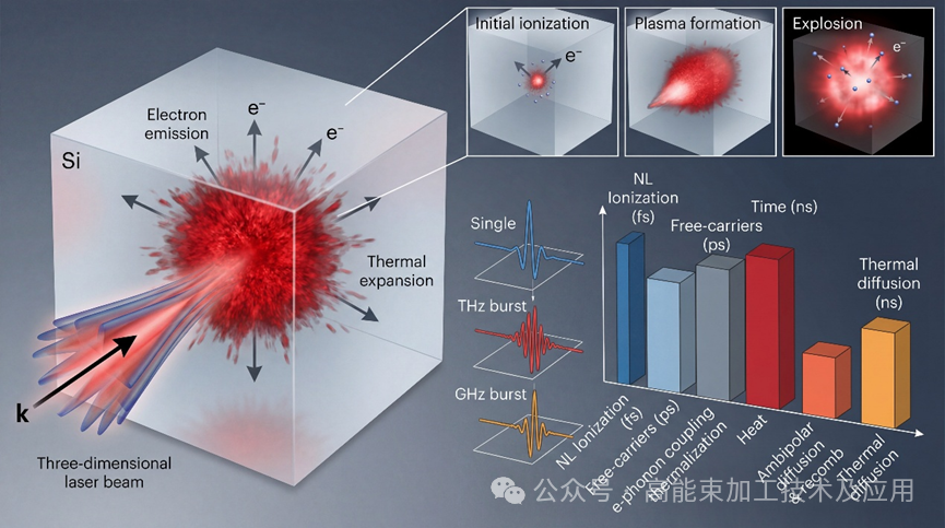
Figure 1. Schematic diagram of nonlinear ionization, plasma evolution and thermodynamic mechanism of ultrafast laser-silicon interaction.
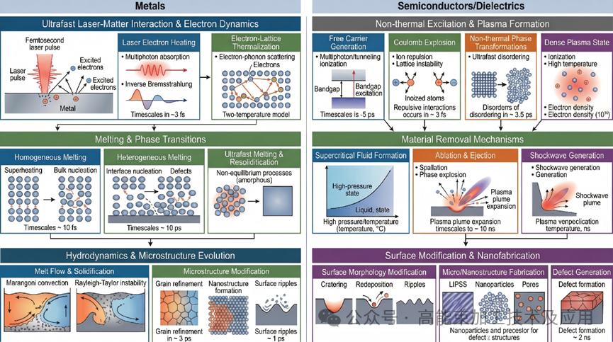
Figure 2. Comparison of energy deposition mechanism and phase transition process of metal and nonmetal materials in ultrafast laser micro/nano welding.
03 Applications of Ultrafast Laser Welding
At present, ultrafast laser micro/nano welding has been widely applied to the interconnection of various conductive micro- and nanostructures. Based on material characteristics, these applications can be broadly categorized into metal micro/nano welding, semiconductor nanomaterial welding, and heterogeneous material heterojunction welding. Across all three categories, ultrafast laser welding demonstrates significant advantages over conventional techniques.
In the precision interconnection of metal micro- and nanostructures, traditional micro-welding techniques often suffer from uncontrolled heat input when processing micron- or nanometer-scale metal wires, leading to severe thermal overflow effects. Excessive thermal loading can easily melt or break fine metal wires and promote the formation of brittle intermetallic compounds at dissimilar metal joints, resulting in low joint strength and frequent defects. In contrast, ultrafast laser welding employs a unique strategy combining high pulse repetition rates with low pulse energy, effectively overcoming these limitations. This synergistic mechanism ensures sufficient energy accumulation for welding while significantly reducing excessive ablation of the metal substrate, thereby suppressing brittle intermetallic compound formation and minimizing weld defects.
In practical applications, researchers first demonstrated dissimilar metal welding between Ag microwires and Cu substrates, confirming its potential for microelectronic interconnects. Furthermore, for nanoscale Ag–Ag homogeneous nanowires, successful welding was achieved using 35 fs pulses at an energy density of approximately 90 mJ/cm². The resulting joints exhibited intact structures, excellent electrical conductivity, and strong mechanical performance.
For damage-free joining of semiconductor nanomaterials, conventional global heating or contact-based welding methods often destroy the crystal structure of nanowires or cause thermal damage to non-welded regions due to the intrinsic brittleness and thermal sensitivity of semiconductors. Ultrafast laser welding addresses this challenge through localized plasma resonance mechanisms. When femtosecond laser pulses irradiate nanowires, localized plasma resonance is induced at crossing points or junctions, generating localized high temperatures for melting, cutting, or reshaping. Owing to the ultrashort interaction time, thermal diffusion reaches equilibrium within the picosecond scale (10⁻¹² seconds), confining high temperatures strictly to resonance regions and completely avoiding thermal damage outside the weld zone.
Based on this mechanism, researchers successfully welded ZnO–ZnO homogeneous semiconductor nanowires using 35 fs pulses at an energy density of 77.6 mJ/cm². After 30 seconds of irradiation, the nanowires formed strong, damage-free joints. This achievement provides an efficient and precise non-contact processing method for assembling all-oxide optoelectronic detectors and sensors.
In the integration of heterogeneous material heterojunctions, joining metals with semiconductors or oxides is essential for constructing multifunctional devices. However, conventional methods struggle to achieve high-quality interfaces due to large differences in melting points and poor chemical compatibility, often introducing high contact resistance. Ultrafast laser micro/nano welding enables high-performance heterogeneous interfaces through localized plasma absorption enhancement. Laser irradiation significantly enhances the local electromagnetic field at the heterojunction, precisely depositing energy at the interface and promoting atomic-level bonding.
Researchers demonstrated that femtosecond laser irradiation at the junction of Au nanowires and TiO₂ successfully induced localized plasma absorption enhancement, forming heterojunctions with both high mechanical strength and high electrical conductivity. This process required only a low energy density of 18.3–21.5 mJ/cm² and an extremely short processing time of 5 seconds. In addition, successful welding of Ag–TiO₂ heterogeneous nanowires further confirms the immense potential of ultrafast lasers in addressing heterogeneous material integration challenges.
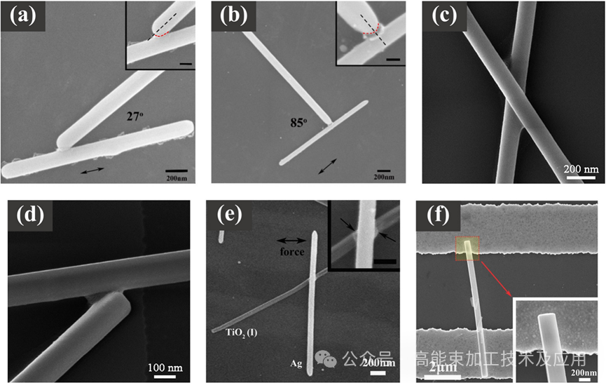
Figure 3. (a, b) are the welding structures of silver-silver homogeneous metal nanowires [1]; (c, d) are the welding structures of ZnO-ZnO homogeneous semiconductor nanowires [2]; (e) is the welding of Au nanowires and TiO2 [3]; (f) is the Ag-TiO2 heterogeneous nanowire [4].
04 Summary
Ultrafast laser micro/nano welding technology, enabled by its ultra-short pulse duration and extremely high peak power, overcomes the limitations of conventional welding methods in thermal effect control and has become an indispensable tool in micro- and nano-manufacturing. By leveraging localized plasma resonance and nonlinear absorption mechanisms, this technology achieves precise melting and bonding at extremely small spatial and temporal scales while effectively avoiding thermal damage to surrounding micro/nanostructures. From metal microwires to semiconductor nanowires and complex heterogeneous material heterojunctions, ultrafast laser welding demonstrates broad material compatibility and excellent processing quality. With continued advances in laser–matter interaction research and further improvements in laser performance, ultrafast laser micro/nano welding is expected to play an increasingly critical role in the fabrication of flexible electronics, nano-optoelectronic devices, and highly integrated sensors, driving micro/nano manufacturing toward higher precision and efficiency.
References:
[1] Lin, L.; Liu, L.; Peng, P.; Zou, G.; Duley, W.W.; Zhou, Y.N. In situ nanojoining of Y- and T-shaped silver nanowires structures using femtosecond laser radiation. Nanotechnology 2016, 27, 125201.
[2] Xing, S.L.; Lin, L.C.; Zou, G.S. Two-photon absorption induced nanowelding for assembling ZnO nanowires with enhanced photoelectrical properties. Appl. Phys. Lett. 2019, 115, 103101.
[3] Lin, L.; Zou, G.; Liu, L.; Duley, W.W.; Zhou, Y.N. Plasmonic engineering of metal-oxide nanowire heterojunctions in integrated nanowire rectification units. Appl. Phys. Lett. 2016, 108, 203107.
[4] Lin, L.; Liu, L.; Musselman, K.; Zou, G.; Duley, W.W.; Zhou, Y.N. Plasmonic-radiation-enhanced metal oxide nanowire heterojunctions for controllable multilevel memory. Adv. Funct. Mater. 2016, 26, 5979–5986.
**--Cite the article published by 高能束加工技术 on December 17, 2025, in the WeChat public account "High-Energy Beam Processing Technology and Applications."